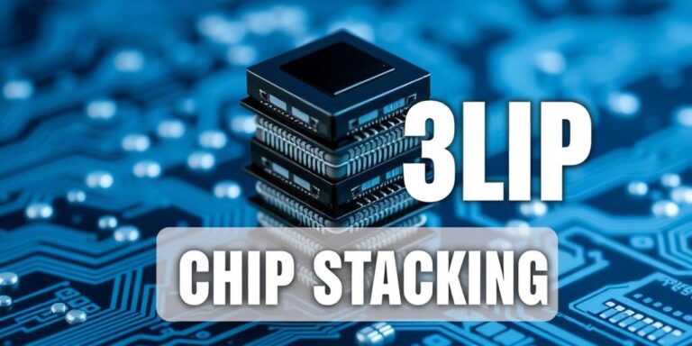
3D Chip Stacking: Vertical Integration for Performance (Post-2025)
As we look beyond 2025, the semiconductor industry is increasingly turning to 3D chip stacking as a key strategy for enhancing performance and density. This approach, also known as vertical integration, involves stacking multiple active layers of silicon to create a single, high-performance chip. This article explores the technology, benefits, challenges, and future prospects of 3D chip stacking.
What is 3D Chip Stacking?
3D chip stacking is a manufacturing process that involves vertically stacking and interconnecting multiple semiconductor dies. Unlike traditional 2D chip designs, which are limited by the surface area of the silicon, 3D stacking allows for a greater number of transistors to be packed into a smaller footprint. This is achieved through various techniques, including:
- Through-Silicon Vias (TSVs): These are vertical connections that pass through the silicon die, allowing for direct communication between stacked layers.
- Hybrid Bonding: This involves bonding the surfaces of two dies together at the atomic level, creating a seamless connection.
- Micro-Bumps: Small solder bumps that connect the stacked dies.
Benefits of 3D Chip Stacking
3D chip stacking offers several advantages over traditional 2D designs:
- Increased Density: By stacking multiple layers, the overall density of transistors and memory cells can be significantly increased.
- Improved Performance: Shorter interconnects between components reduce latency and improve overall performance.
- Reduced Power Consumption: Shorter interconnects also reduce power consumption, making 3D chips more energy-efficient.
- Heterogeneous Integration: 3D stacking allows for the integration of different types of dies (e.g., CPU, GPU, memory) into a single package, optimizing performance and functionality.
- Smaller Form Factor: Stacking components vertically reduces the overall footprint of the chip, which is crucial for mobile and other space-constrained applications.
Challenges of 3D Chip Stacking
Despite its potential, 3D chip stacking also presents several challenges:
- Thermal Management: Stacking multiple layers increases the density of heat sources, making thermal management more difficult. Effective cooling solutions are required to prevent overheating and ensure reliability.
- Manufacturing Complexity: 3D chip stacking is a complex manufacturing process that requires precise alignment and bonding of the dies. This increases manufacturing costs and reduces yield.
- Testing and Reliability: Testing 3D chips is more challenging than testing 2D chips, as it is difficult to access the internal layers. Ensuring the reliability of the stacked dies over time is also a concern.
- Cost: The advanced manufacturing techniques and materials required for 3D chip stacking can make it more expensive than traditional 2D designs.
Future Prospects
Looking ahead, 3D chip stacking is expected to become increasingly important for high-performance computing, artificial intelligence, and other demanding applications. Several trends are driving the adoption of 3D chip stacking:
- Increasing Demand for Bandwidth: As data rates continue to increase, 3D stacking offers a way to provide the necessary bandwidth for high-performance computing.
- Growing Complexity of Applications: AI and machine learning applications require massive amounts of computing power and memory, which can be better addressed with 3D chip stacking.
- Advancements in Manufacturing Technology: New manufacturing techniques, such as hybrid bonding and advanced TSV processes, are making 3D chip stacking more cost-effective and reliable.
- Industry Collaboration: Collaboration between chipmakers, equipment manufacturers, and research institutions is accelerating the development and adoption of 3D chip stacking.
Conclusion
3D chip stacking is a promising technology that offers significant advantages in terms of density, performance, and power consumption. While there are still challenges to overcome, ongoing advancements in manufacturing technology and increasing demand for high-performance computing are driving the adoption of 3D chip stacking. As we move beyond 2025, it is likely to become an essential technique for enabling the next generation of electronic devices.